Converting a Tektronix 7T11 to a 7T11A
In the spring of 2011 I bought a couple of Tektronix 7854 oscilloscopes, which are very fine mixed mode (Analogue and DSO) oscilloscopes. These work well with most of the 7000 series plug-ins, but not with the 7T11 Sampling Sweep Unit. Tektronix brought out a revised version of this timebase called the 7T11A which had circuit modifications and additional circuitry to create the special blanking signals that are required for it to work with the 7854. Unfortunately, not many 7T11A Sampling Sweep Units appear on the second hand market, and when they do they command very high prices.By the end of November 2011 the 7854s had been "brought back from the dead" and were working well. I was looking for a project and decided that I would try to convert my 7T11 to a 7T11A.
Ordering
The project was a success, and a kit of parts for the blanking board is now available at a cost of GBP50.00 including postage (International Signed For, or AirSure). If you live in the UK, the cost is £40.
I'm sorry for the recent price increase, but I can't continue to
subsidise the large increases in postal charges. To order
the kit, please email
me.
First steps
The first place to look for information on what changed between the 7T11 and the 7T11A is the supplement at the back of late 7T11 service manuals which were released before a proper 7T11A service manual was issued. I also found a copy of the 7T11A service manual to be invaluable as there turned out to be a number of errors in the supplement.
You can download the supplement from 7T11A Modification Insert.
I soon found by comparing the list of parts in the supplement and
that in the main body of the manual that most of the changes were
trivial. For example: changing the voltage rating of a
capacitor from 1000V to 100V in circuit that would never see more than
15V, or from a 1/8W carbon composition resistor to a 1/4W part with
the
same value, or replacing a germanium diode with a silicon schottky
diode. The only significant changes appeared to be those that
were in the ADD: or REMOVE: portions of the changed parts list, and
those that were covered on page 9 and following in the supplement.
The substantive changes are the addition of a new blanking signal circuit to the Analog Logic board to provide the additional signals required by the 7854, and the changes needed to provide the signals from other parts of the plug-in to the new circuit. A few other relatively trivial circuit changes also appear to have been made between the 7T11 and the 7T11A, but are not critical to supporting the 7854. I will mark these as optional changes in what follows.
The new blanking circuit
This is shown on page 11 of the supplement and on schematic
<7> "Slow Ramp Generator and Output Amplifier" in the 7T11A
Service Manual. A close inspection of the two schematics shows
that they differ. I didn't pick up this difference until I'd
had
the first batch of PCBs made based on the schematic in the 7T11A
manual, and they didn't quite work right! With the invaluable
assistance of Albert
Otten who owns a real 7T11A, it was fairly soon established that the
schematic in the supplement is correct, and the one in the 7T11A
Service Manual is in error. CR4
(a 1N4152 diode) is shown connected the wrong way up. The
cathode
should
connect to ground and the anode to the base of Q5.
Here is the re-drafted schematic with modifications to use mostly surface mount parts that was used for the PCB design. I used mostly the same parts as the original except in surface mount form (e.g. MMBT3904 instead of 2N3904). I used a PN4250A for Q8 instead of a PN4250 (just a voltage rating difference), and substituted an HSMS2810 for CR5 and an MMBT5771 as the closest surface mount cross for Q1 which was originally a PN4258.
7T11A blanking
board schematic
Modifying your 7T11
Preparing your 7T11 to accept the new 7854 blanking board
Here is a full set of changes including those I consider optional (which I haven't made in all cases) to convert a 7T11 to a 7T11A and to install this new PCB.
- Remove the trigger board and the timing board
- (Optional) in the x10 trigger input amplifier on the trigger board, remove R92 (68 ohms) and replace it with a 130 ohm 5% 1/8W carbon composition resistor. You could probably use a thick film surface mount resistor here if you wanted to make this change (which I think improves the HF response of the circuit) as these are also low inductance parts.
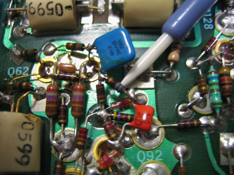
- On the timing board, carefully remove CR368 (1N4152), R362 (4K7) and TP368. Note that the schematic shown on page 13 of the modification supplement is in error: It incorrectly shows a connection between the emitter of Q362 and the base of Q368 which should not be there.
- Install the 4K7 resistor removed in step 2) above to replace CR368
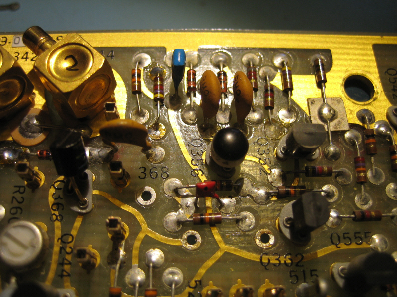
- Remove R365 (39K) and R366 (43K)
- Cut the trace between the collector of Q244 and the collector of Q368.
- Replace R365 with a 47K part, ideally using a 47K 1/4W or 1/8W
carbon composition part. I got lucky, R366 which was nominally 43K
had drifted high, so I was able to re-use this to replace R365.
Also install one end of a 20K resistor into the same hole in the PCB as R365 goes into (thus connecting it to the base of Q368). Solder a 30cm (1 foot) length of wire (I used blue) to the other end of the resistor and cover the section with the resistor in heat shrink to prevent shorts. Dress the wire along the length of the timing board and down through the hole by the silkscreen legend +15V so it can be connected to TP106 on the trigger board at a later stage.
- Replace R366 with a 51K resistor.
- On the back of the timing board install the diode removed in step 2) with the anode connected to the base of Q368, and the cathode (black band end) connected to the solder pad just below the through board connector "CJ" which is to the lower left of Q368 (as viewed from below). To aid in identification, this is also the top end of R241. This is where the Real Time/Equivalent Time signal enters the Timing Board from the Interface Board.
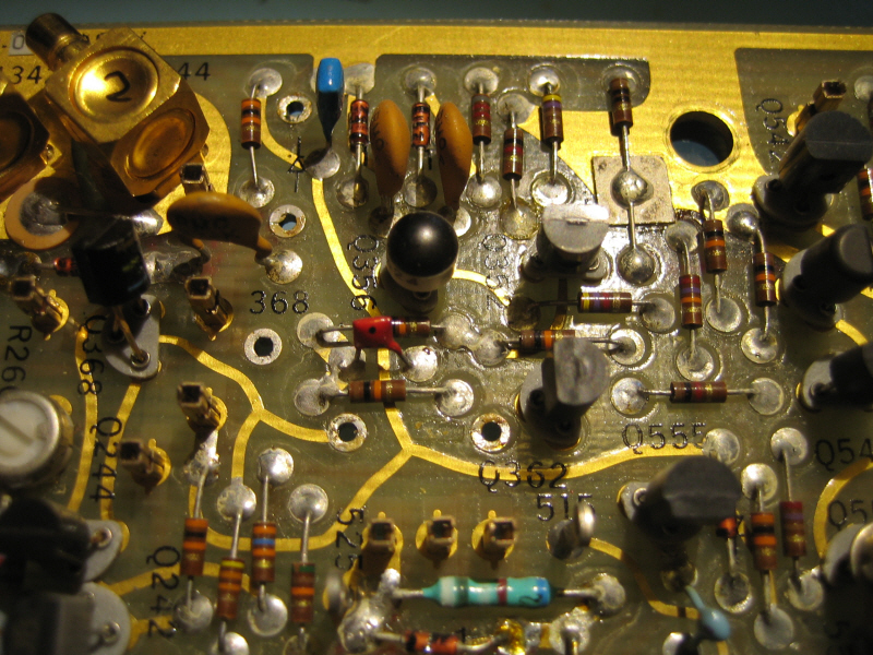
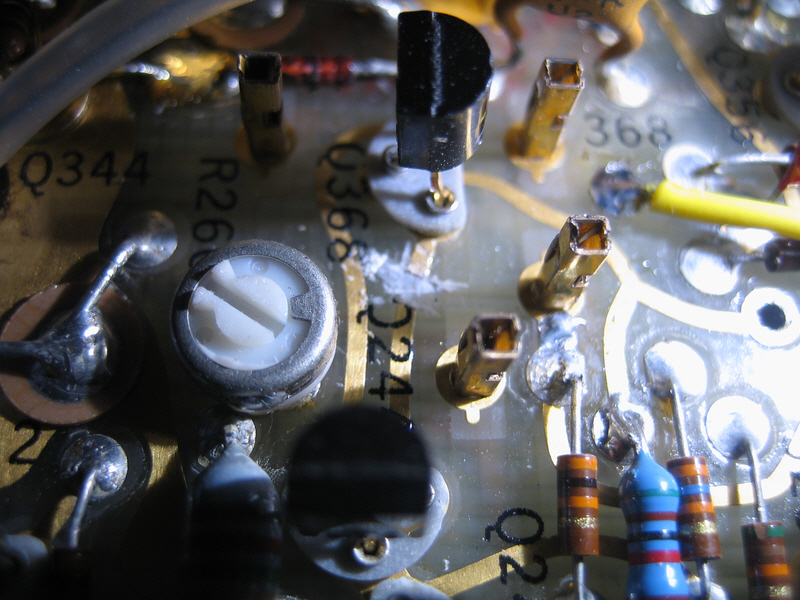
- Cut all the traces running from interboard connector "CI" (which
run to R368, the hole where TP368 was installed and the collector of
Q368). This isolates the interboard
connector.
Run an EC wire (I used black) from the collector of Q244 to
interboard
connector "CI" (which eventually connects to A1 on the rear edge
connector).
Install EC wires (I used white) from the collector of Q368 to the hole where TP368 was, and from there to the lower end of R368.
- Install a 1N4148 diode with the cathode connecting to the top of R368 and the anode to interboard connector "CI". This is the new CR368 (see 7T11A Schematic <3> "Time to Height Converter") connecting between the collector of Q244 and +5V at the top of R368.
- Connect a yellow wire of about 30cm (12") length to the hole in the board from which TP368 was removed, dress this along the board with the blue wire, and then feed it over the top of the interface board alongside the existing cable bundle (this will eventually connect to pin 4 of J1 on the added 7854 blanking board).
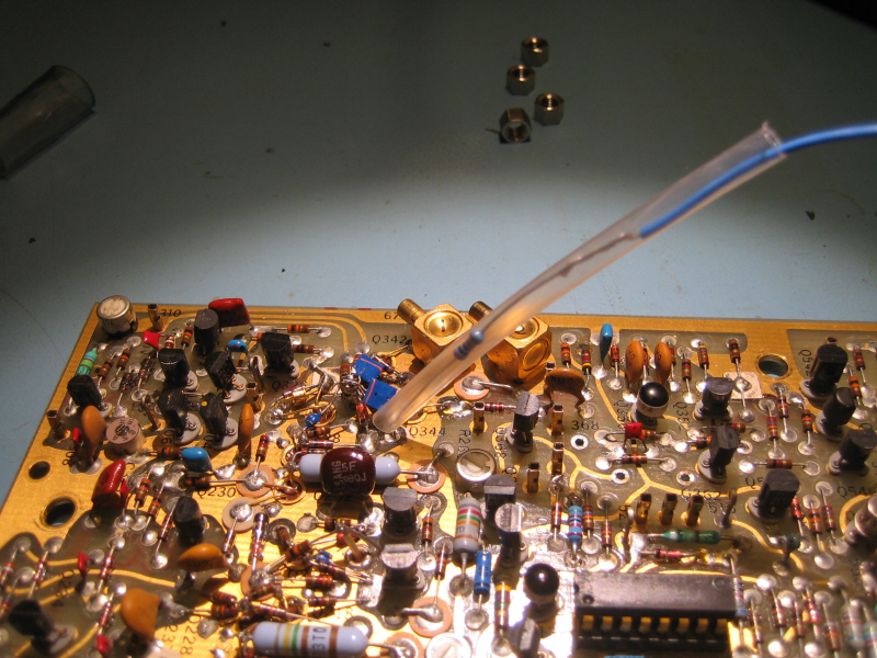
- Re-install the timing board.
- (Optional) on the trigger board, change C182 from 47pF to 22pF.
- Re-install the trigger board, thread the blue wire up through the hole to the right of P101, leaving a few inches slack, and connect the end to TP106
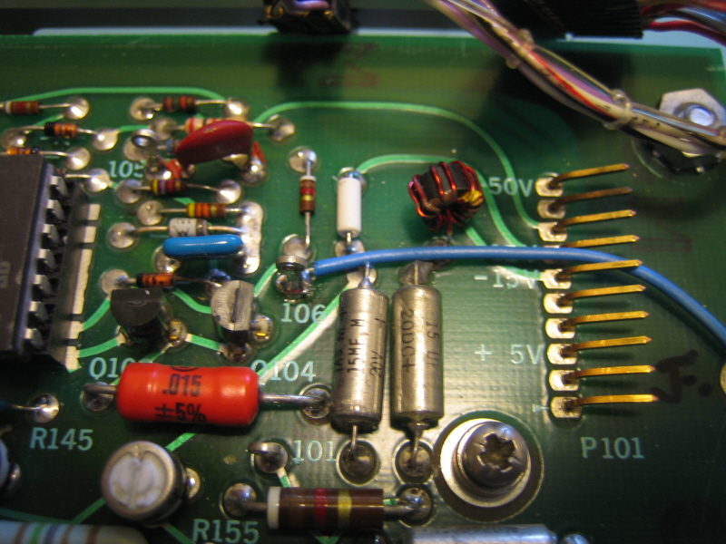
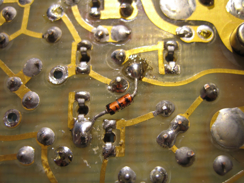
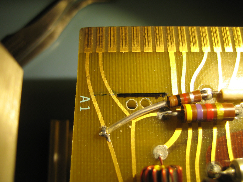
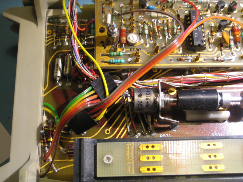
- On the Analog Logic Board, cut the trace between the top of R671 and the emitter of Q668. The cut is clearly shown in the first picture after step 18.
- Cut a 5" (125mm) length of 3 way ribbon cable (I used colour coded - Brown, Red, Orange), trim the yellow wire (from step 8 above) to length and make up a four way push on 0.1" pitch connector. This will connect to J1 on the new blanking board.
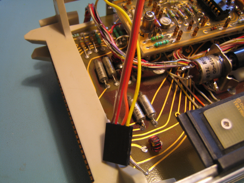
- Assuming that you have wired the connector
1=Brown, 2=Red,
3=Orange, 4=Yellow, connect the brown wire to a convenient ground
point. On the 670-1118-07 revision of the logic board installed in
my
7T11, the pad just to the right of CR596 was vacant so I used
that. Note that CR597 shown in the 7T11 manual was replaced by
a
jumper at revision code 04 of the logic board.
Warning: This pad will not be a ground connection on earlier board revisions, so you'll have to connect to another ground point.
Connect the red wire to +5V at the left hand end of R668, and the orange wire to the top end of R671.
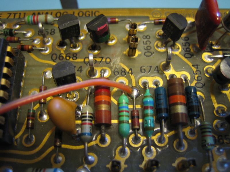
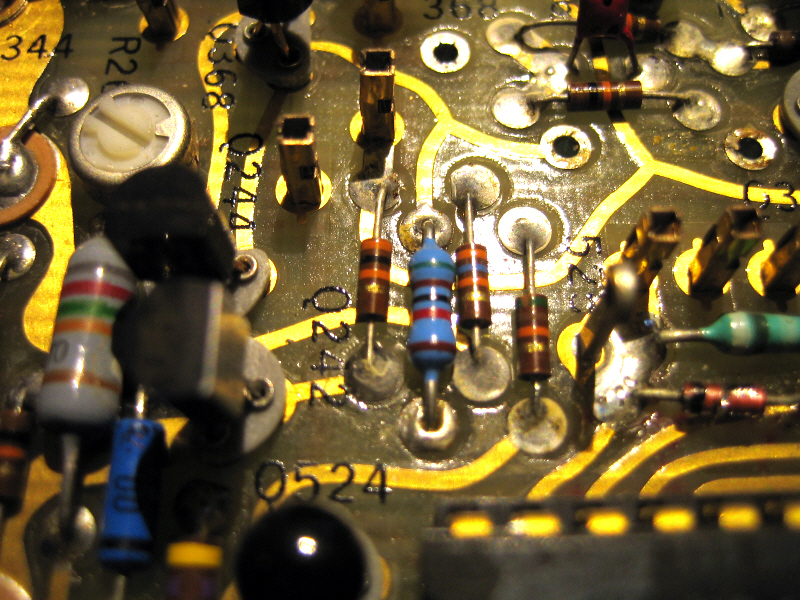
- (Optional but recommended) On the Analog Logic board, remove C630 (220pF) which is just below Q364, and replace with a 100 ohm resistor (R630 added) in series with a 200pF (C630 replaced) capacitor.
- Cut a 3" (75mm) length of 5 way ribbon cable. Make up a 5 way push on 0.1" pitch connector 1=Brown, ... 5=Green.
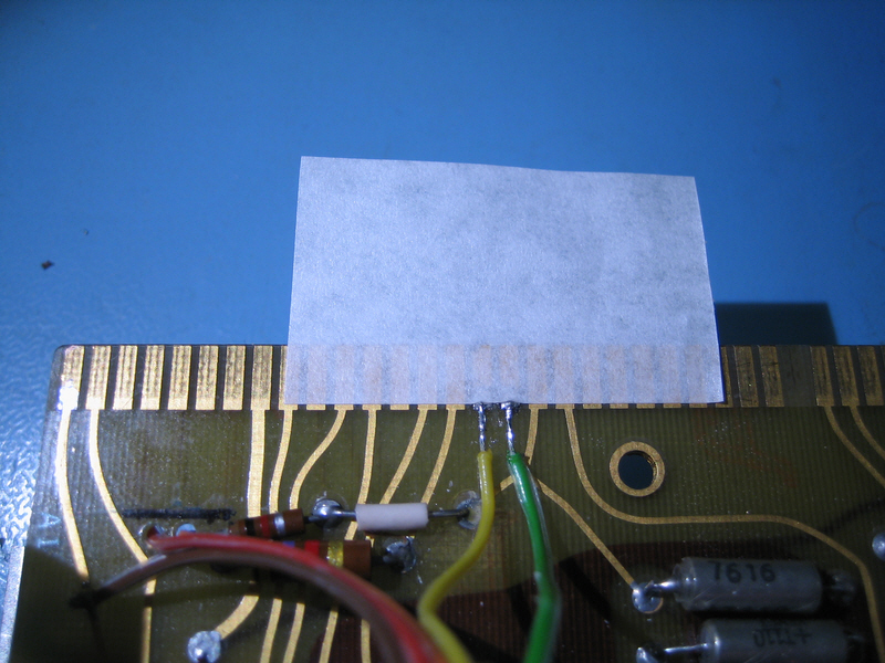
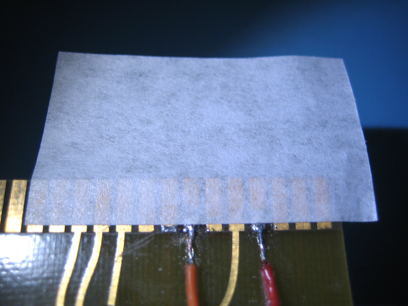
- Using the rear plastic moulding as a guide, mark the interface board (A3 - A7 area) to show the location of the edge of the moulding and then remove the moulding. Drill two 2mm holes just forward of the line you marked at about the level of A3 and A4. Take care that you don't drill through the trace going to B5 on the other side of the board.
- Make clearance notches in the plastic moulding to allow the wires to pass to the pads A1, B4, B7, A16, A17. I used a fine pointed soldering iron tip.
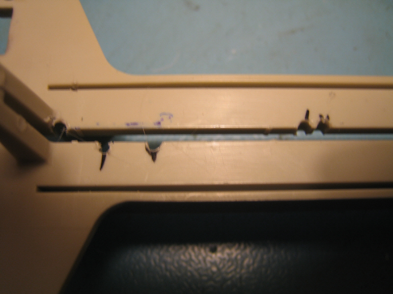
- Split out the ends of the 5 way ribbon cable to 1.75" (45mm). Strip about 3/16" (about 5mm) of each and solder the wires as follows: Brown to the trace leading to pad A1 at the point where the resistor connects, Red to B4, Orange to B7, Yellow to A16, and Green to A17. Use masking tape to protect all but the rear 1mm or so of the edge connector pads.
- Re-install the rear plastic moulding.
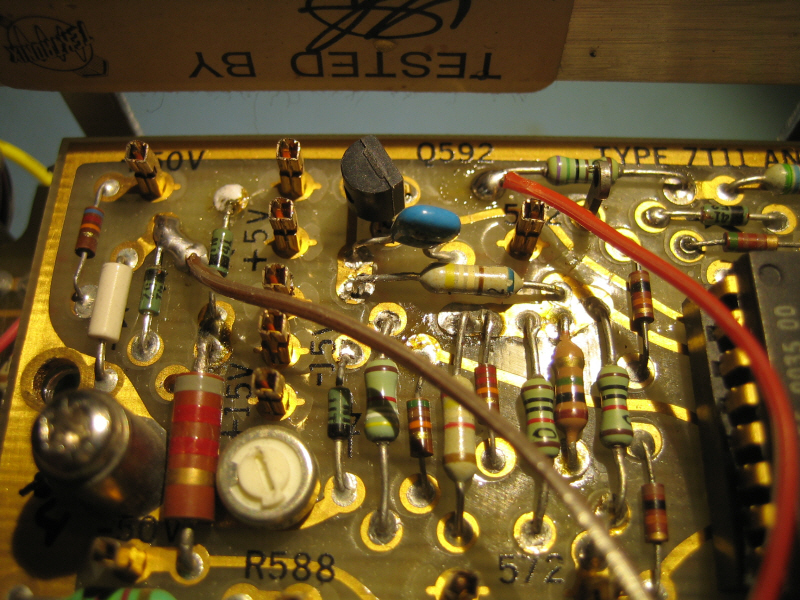
- (Optional) On the Analog Logic board, install a 1nF (nominally
100V) capacitor C676 between inter-board connectors "BJ and "R"
(bottom ends of R676 and R686). Note that the
instructions
and the schematic on page 16 of the supplement are incorrect.
The
7T11A schematic <7> "Slow Ramp Generator & Output
Amplifier"
is correct.
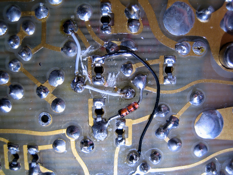
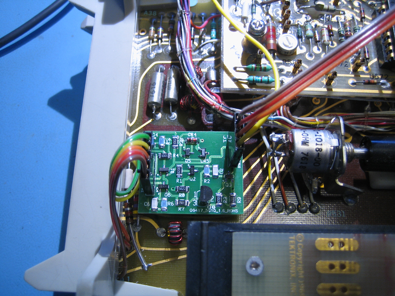
Building the 7854 blanking PCB
Here's what the bare PCB looks like:
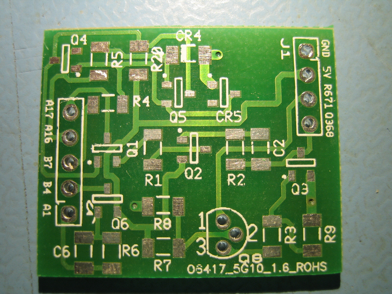
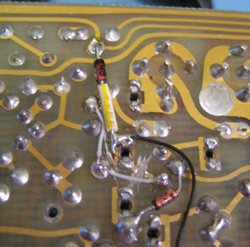
There's not really a lot to say about putting it all together,
expect that you should make
sure you install diode CR4 (a MELF 1N4152) which is at the top centre
of the board the right way round. The photograph of the
PCB
above shows it with the cathode to the left (as does the next
photograph). That is incorrect. The cathode should
be
on the right (connected to
ground).
If you don't have much experience of surface mount soldering, it's worth taking a look at the video tutorial entitled Surface Mount Soldering 101 which you will find at:
http://www.curiousinventor.com/guides/Surface_Mount_Soldering/101Once you've put the board together all that remains is to secure it in place on top of the two metal tantalum capacitors using some "Blu-Tack" or similar, and connect the push-on connectors to the headers.
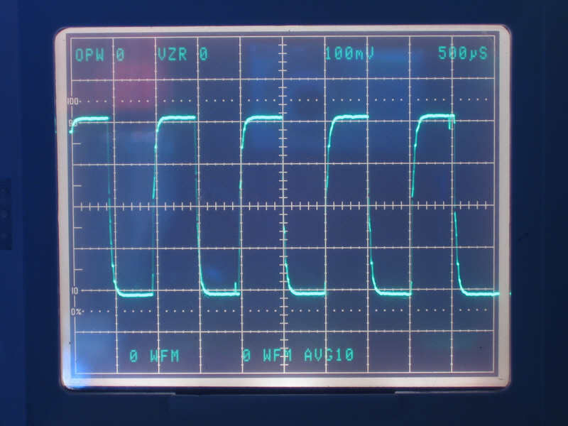
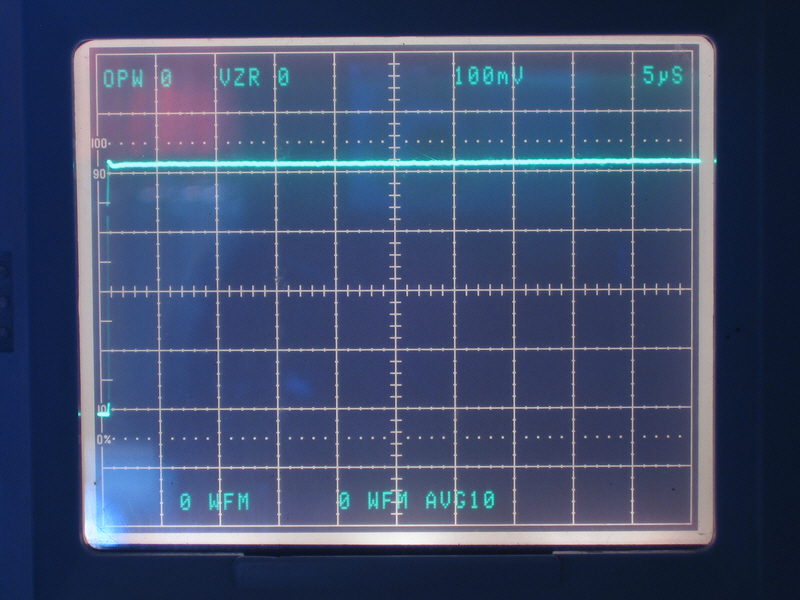
The proof of the pudding
Here are a couple of screen shots taken with the modified 7T11 installed in a 7854. The first is a 10 waveform average of the calibrator output in "real time" sampling mode at 500uS per division, while the second is a 10 waveform average of the calibrator output in "equivalent time" mode at 5uS per division.