Frequency Divider Design for a GPSDO
This was available to buy as a made up circuit board, but they've all been sold. I don't expect to be making any more of them unless I get around forty people banging on my door wanting them. If you want the Gerber files for the four layer surface mount PCB please email me.
Introduction
A GPS Disciplined Oscillator typically produces a 10MHz output. It is often useful to have additional frequencies that are a sub-multiple of the 10MHz signal available.I wanted a frequency divider that would provide low jitter or phase noise when fed with the output of a Trimble Thunderbolt GPS disciplined oscillator. The 10MHz output of the Thunderbolt is a sinusoidal signal at a level of +12.5dBm +/- 2.5dBm into 50 ohms. This is about 2.5V peak to peak.
I decided that I wanted to provide square ware output signals at 10MHz, 5MHz, 1MHz, and one output with the output frequency selectable from 100kHz to 1Hz in decades. The output level should be 5V into 1MOhm and 2.5V into 50Ohms.
I am indebted to Bruce Griffiths and others on the “time-nuts” mailing list for assistance with and constructive criticism of the design. All faults are my own (with a little help from the schematic capture and layout software).
Design for the input clock shaper.
The main divider circuit requires a 10MHz square wave input clock signal at CMOS signal levels. The Trimble Thunderbolt output is a sine wave at about 2.5V peak to peak. So it is necessary to use a clock shaper circuit to convert the input sine wave to a square wave clock signal. The design used is a capacitively coupled input driving an ADCMP600 or MAX999 comparator (either may be used). The design is from Bruce Griffiths’ web page on clock shapers:http://www.ko4bb.com/~bruce/CLKSHPR.html
The circuit has a wide bandwidth [<10kHz, > 100MHz], and the input amplitude range is [100mV - 5V]p-p.
The clock shaper circuit was originally designed for use in a linear phase detector, but there are many other applications for which it is suitable. It is derived from the input clock shaping circuit in the HP K34-5991A. An ADCMP600 (or MAX999) comparator with a CMOS/TTL compatible output is substituted for the ECL differential amplifiers in the K34-5991A.
Design for the frequency divider.
The schematic is here: Frequency Divider 2.1 Schematic.pdfThe frequency divider is based around the use of a 74AC163 counter configured to divide by ten to derive the 5MHz and 1MHz output signals. The 74AC163 was chosen in preference to the 74HC163 as the chip delays are lower in the 74AC163. The lower frequency signals are derived from the 1MHz output of the 74AC163 using a chain of 74HC4017s.
The 5MHz output is taken directly from the QA output of the 74AC163 and reclocked to the 10MHz clock signal using a 74AC74 D-type flip-flop. The signal is re-clocked in the second half of the 74AC74 to delay the signal by one additional 10MHz clock cycle.
The 1MHz signal is derived from the “Ripple Count Out” (RCO) output of the 74AC163. This signal is a pulse signal, not a square wave. This is converted to a square wave using a 74AC164 shift register (serial in parallel out) and a 74AC112 JK flip-flop. The signal is then re-clocked in the other half of the 74AC112 to delay the signal by one additional 10MHz clock cycle.
The double clocking of the 5MHz and 1MHz outputs is so that the rising edges will be aligned with the rising edges of the low frequency outputs, the derivation of which is described below.
The 1MHz output is further divided down by a chain of six 74HC4017 Johnson Counters connected as a ripple divider which provides outputs from 100kHz down to 1Hz. A 74HC4051 analogue multiplexor is then used to select one of these outputs based on the input from a BCD thumbwheel switch (such as you might use for setting a SCSI id).
Because the worst case delay through the chain of 74HC4017s will not allow all the possible outputs of the 74HC4051 to be re-clocked reliably to the same rising 10MHz clock edge as the 5Mhz and 1MHz signals, the output is initially re-clocked to the 1MHz signal used as input to the divider chain, and then to 10MHz. Separate 74AC74 D-flops (U18 and U19) are use to avoid cross modulation.
A dedicated output flip-flop package is used for each output frequency to avoid problems with simultaneous switching of two sets of logic in the same package.
The output stages
The outputs are driven by 74AC541 bus drivers. Four of the eight gates in each package are used. A 180 ohm resistor is used in series with the output of each gate, and the outputs are then commoned. The value of 180 ohms was chosen rather than 200 ohms because the 74AC541 output stages have non-zero output resistance, typically in the region of 25 ohms plus or minus 50%. This gives a close match to a 50 ohm load.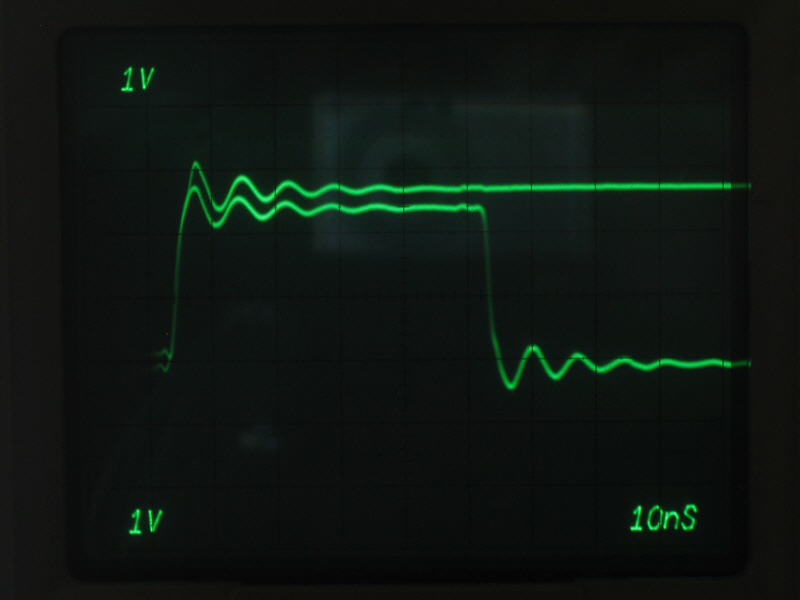
As you can see from oscilloscope screen shot above, the output has quite noticeable overshoot. If this is not acceptable, then it has been suggested that you may wish to try using 74AHC541s as the output drivers instead of 74AC541s. If you do so, you may also wish to change the output series termination resistors to 150 ohms.
Construction notes
and purchasing information
As this design used mostly surface mount parts, a completely built PCB
with the exception of the RF input and output connectors was available
at a cost of GBP75 including shipping to anywhere on the
planet. A photograph of the board is shown below: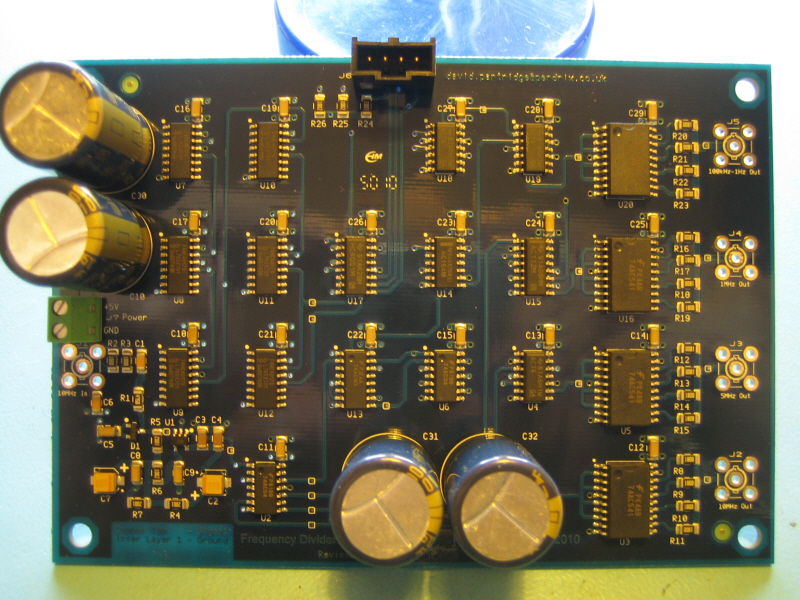
All resistors used in the design are Stackpole RNCP size 1206 thin-film surface mount 0.5W parts. Thin film parts were chosen for reduced flicker noise. All ceramic capacitors are X7R. It has been suggested that there may be some benefit in using C0G (NP0) parts in the input clock shaper circuit, but this has not been tested.
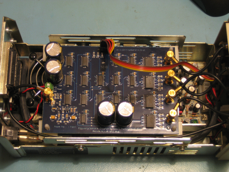
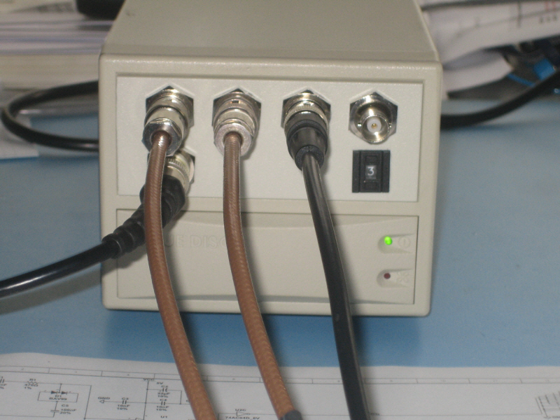
For my own use I housed the board in an old 3.5" external SCSI enclosure, and here are a couple of pictures showing what it looks like:
Test results and Power Supply considerations
Testing was done with the 10MHz input driven from my Trimble Thunderbolt. Jitter on the input sine wave was less than I am able to measure (certainly below 100pS).Running the divider from a switch mode supply with about 2mV of approx. 1kHz (variable) "spiky" ripple plus about 1mV of RF "hash". I see about 1nS jitter on the rising edge, while on the falling edge it is closer to 2.5nS to 3nS. This jitter is present on the output pin (Pin 1) of the comparator. The remainder of the board seems to add no additional jitter.
Substituting a reasonably clean linear supply with about 0.1mV noise on the 5V supply gives much better results: Jitter is still present but down to about 100ps to 150pS for the rising edge, and between 225 and 250pS on the falling edge of the signal at the output pin of the comparator. As before the remainder of the circuit seemed to add no additional jitter.
An additional test was performed with the switching supply but this time a small common-mode choke was inserted in the supply lines just before the connections to the PCB. This improved the jitter considerably with results comparable to those achieved with the linear supply.
The moral would seem to be that the level of jitter (and hence phase noise) in the output signals is primarily dependent on the quality of the power supply. Use a well regulated and quiet linear supply if at all possible, and use common mode noise filtering as well.
Design change history
| April 2008 |
Original PCB Design |
| 19/08/2008 | Fault: Pin 1 of U18 and Pin 1 of
U19 are not connected to Vcc even though the schematic shows they are. Action: Delete these connections in the schematic, and redraw them. Forward annotation was used to correct the netlist. Draw traces to finalise change. |
| 19/08/2008 | Fault: 5MHz output is 180
degrees out of phase. Action: Drive D input of 2nd flip-flop in U4 from Q output of 1st flip-flop instead of ~Q. |
| 19/08/2008 | Fault: Lower end of C5
(connected to the BAV99 diode clamp) should connect directly to ground, and is instead connected to the screen of the 10MHz input. The impact of having it connected to the input screen is that any low frequency noise on the input signal connector coax shield due to ground potential differences will modulate the diode clamp voltage developed across C5. If the input is sufficient to activate the diode clamps this will add low frequency noise to the input signal at the comparator input. Furthermore, if there is a substantial low frequency difference in the potential of the connector shell and the PCB ground plane, the comparator input protection may fail. The rejection of any such AC potential difference is also significantly worse than when C5 is returned to the PCB ground plane. Action: Connect bottom of C5 in clock shaper to ground plane rather than to input screen. |
| 15/03/2010 | Improve LF rejection: Replace
C10 (47uF) with 6,800uF capacitor, add three additional 6,800uF capacitors (C30, C31, C32) |
| 15/03/2010 | Replace J7 (Power input connector) with Phoenix 3.81mm screw connector |
| 07/04/2010 | Revision 1 PCB |
Documentation
Schematic: Frequency
Divider 2.1
Schematic.pdf Current PDF Version of writeup: Frequency Divider 2.1.pdf
Current Bill of Materials: Frequency Divider 2 Bill of Materials.xls
2008 PDF version of writeup: Frequency Divider 2.pdf
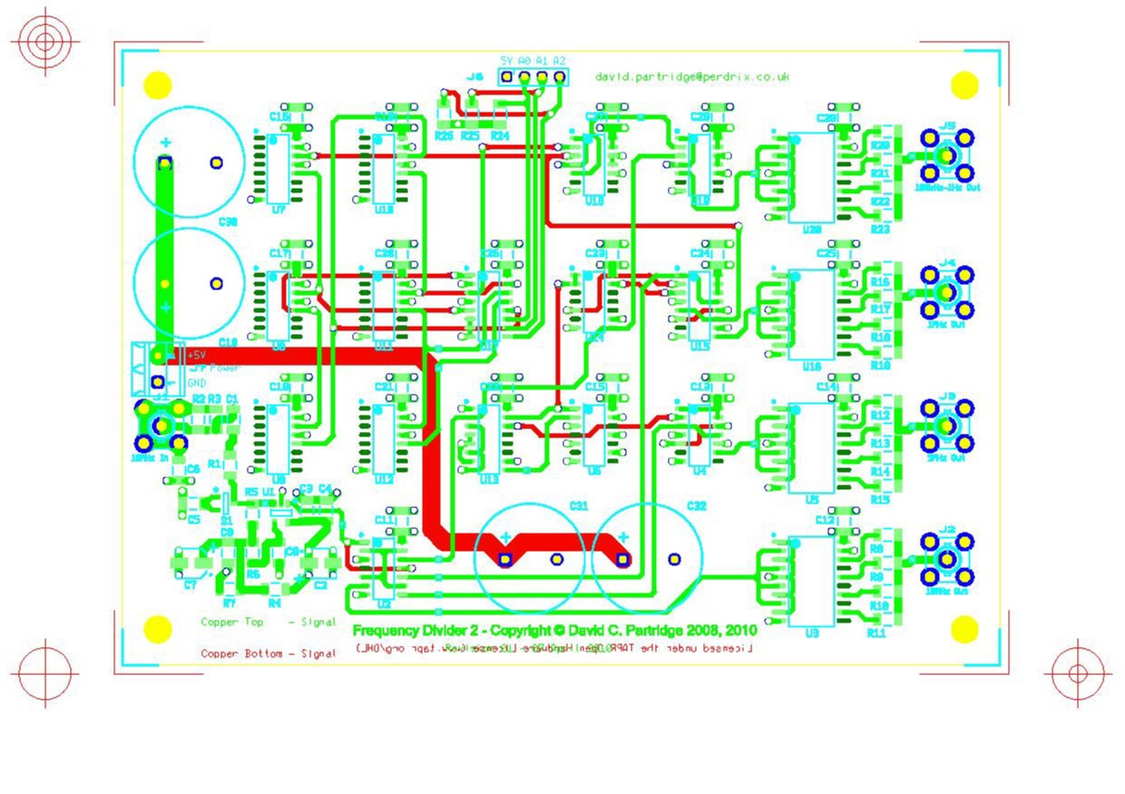
Top and bottom layers of the board are shown below (inner layers not shown):
LICENSED UNDER THE TAPR OPEN HARDWARE LICENSE (WWW.TAPR.ORG/OHL)
© David C. Partridge 2008, 2010
